

Step 1: Rectification of Mains Voltage
At the input of an AC/DC power supply, a 1-, 2- or 3-phase mains voltage (AC) is present. For simplicity, the functionality is explained using the example of a 1-phase 230V (50Hz) voltage. The diode is the crucial electronic component for rectification. It is only conductive in one direction, the other direction is blocked. Like a check valve.
Since only one half-wave is generated with just one diode (left image), which wastes a lot of energy, this is optimized using the full-wave rectifier method (right image).


Step 2: Voltage Smoothing with Mains Filter
However, the voltage is not yet permanently available; it also drops to 0V. The constant switching on and off would heavily stress a connected electronic circuit.
To fill these "voltage gaps" or to buffer them, a passive 2nd order low-pass filter is used in this example. The capacitor C stores the voltage or is charged and then releases it again when our supply voltage decreases. The storage choke keeps the current flow almost constant. How far the voltage drops depends on the size of the capacitor and the flowing current.

Step 3: DC Input Voltage Conversion
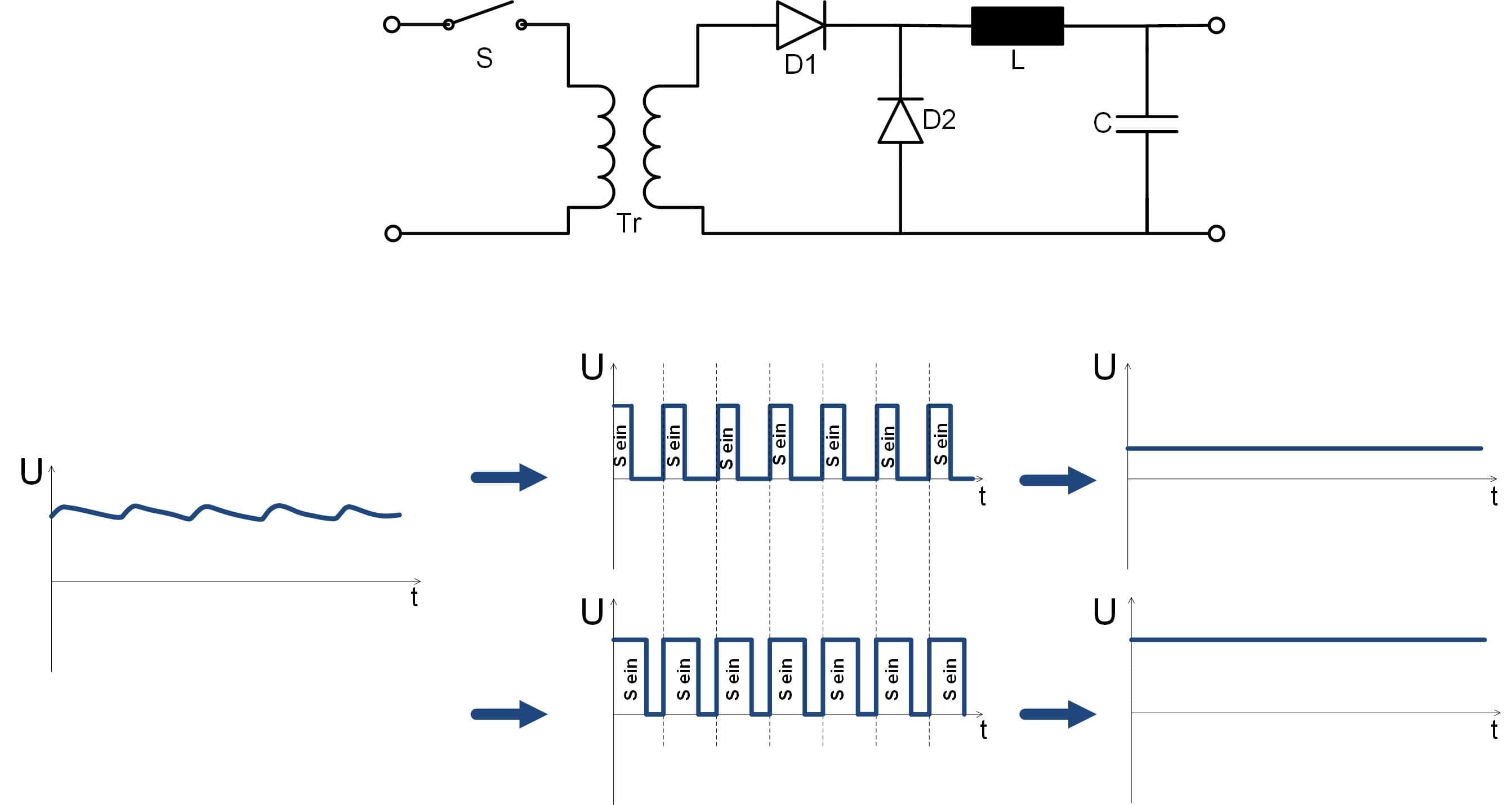
Now the rectified, smoothed mains voltage (approx. 325V) must be converted to the desired output voltage value. A DC/DC conversion takes place. In this example (Figure 3), the circuit topology of the forward converter is chosen. However, other topologies are also possible.
The switch S corresponds to a switching transistor, which is controlled by a control unit (not shown) with switching frequencies from a few 10 kHz to a few 100 kHz and load-dependent pulse widths.
The transformer Tr provides galvanic isolation and converts the input voltage to a secondary-side voltage according to the turns ratio.
Conducting State
In the conducting state, when switch S is closed, a current flows through the primary winding of transformer Tr and a current translated by the turns ratio flows through output-side diode D1 and storage inductor L. Diode D2 blocks in this state. Due to the buildup of a magnetic field in the storage inductor, the current increases linearly. Capacitor C is charged to the output voltage. Energy transfer occurs during the conducting phase.
Blocking State
In the blocking state, switch S is open and D1 blocks because the secondary voltage reverses polarity. The storage inductor L enables a continuous current that flows through the then conducting D2 during the blocking phase. Together with capacitor C, the output voltage UA is kept constant, except for a small ripple.
The output voltage is load-dependent and must be regulated via feedback and control of the switching transistors (not shown in Figure 3).
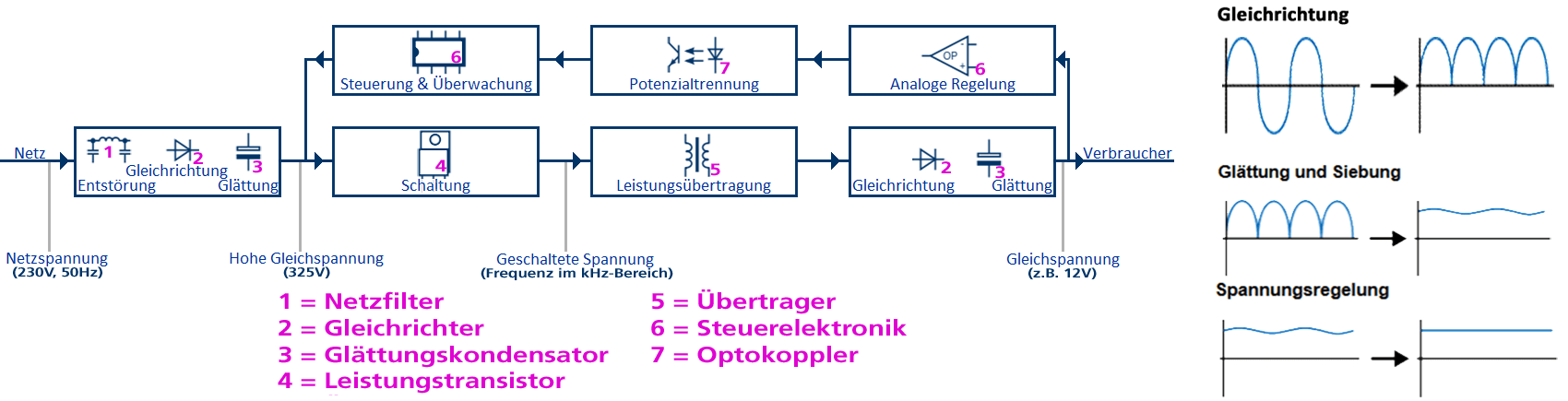
Figure 4: The interaction of the individual steps of voltage conversion is summarized in the block diagram. This representation also includes the feedback of the control unit.